

I. Introduction
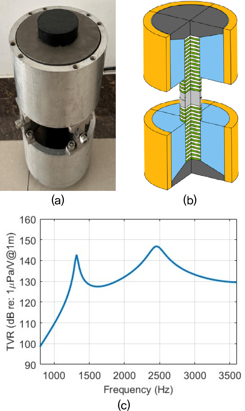
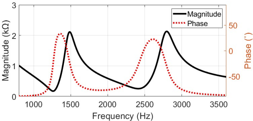
The demand for underwater transducers capable of delivering low-frequency, broadband, and high-power performance is steadily increasing across various applications, including marine environmental monitoring, deep-sea exploration, and sonar surveillance systems.[1,2,3] Among diverse transducer designs explored to meet these requirements, the Janus Helmholtz transducer (JHT) has attracted significant attention due to its simultaneous wideband and high-power capabilities.[3,4,5] The JHT, illustrated in Fig. 1, comprises two symmetrically arranged Tonpilz transducers within a cylindrical metal housing, utilizing both the longitudinal resonance of transducer elements and the cavity resonance of the fluid medium. This configuration enables a high Transmitting Voltage Response (TVR) across a broad frequency range. TVR, representing the transducer’s transmitting efficiency, is defined as the emitted sound pressure level per unit input voltage, typically measured at 1 Vrms. Despite these advantages, the JHT exhibits a notable phase mismatch between voltage and current at frequencies other than resonance points, causing increased reactive power and limiting effective high-power transmission. For example, Fig. 1 illustrates that although the TVR remains practically above 127 dB within the frequency band between two resonances, the voltage-current phase difference peaks around 77.8°, complicating wideband power transfer.
To address these limitations, impedance matching circuits are commonly employed. Traditional matching circuits generally correct phase mismatch via resonant circuits or compensate for transducer capacitance using transformer inductance.[5,6,7] Such circuits primarily optimize power factor at the input impedance but are effective mainly near resonance frequencies, restricting their applicability to non-resonant frequency bands of the JHT. Furthermore, high inductance requirements lead to larger physical sizes and increased manufacturing costs.
Similarly, in the field of impedance matching for dual-resonance transducers, methods have been proposed that integrate multiple resonant circuits to optimize impedance at discrete frequencies.[8] However, these methods also fail to effectively account for interactions between the circuits, thereby limiting their performance in wideband applications.
In addition, to overcome the bandwidth limitations of passive circuits, recent studies have integrated active components into impedance matching circuits that dynamically adjust the input voltage phase.[9] While such active circuits can significantly improve broadband efficiency, they require complex control logic and additional measurement instrumentation to handle the nonlinear load characteristics of transducers.
Recently, a design approach has been proposed that utilizes a simple-structured impedance matching circuit to maximize both input and load power factors for wideband power transfer.[10] While this method can significantly improve broadband power transfer efficiency, it is not optimized from the perspective of maximizing the effective power delivered to the load.
This paper proposes a structurally simple impedance matching circuit designed to maximize power transfer in the JHT. The proposed circuit comprises two resonant subcircuits, each consisting of inductors and capacitors, enabling wideband impedance matching without additional external devices while maintaining low design complexity. The design process involves two primary steps: initially calculating the output and load impedances within the driving system, followed by employing an optimization algorithm to select the optimal component values that maximize active power across the operational frequency range. The effectiveness of the proposed circuit is validated through simulation assessments, demonstrating its ability to significantly enhance power transmission in the JHT.
II. Impedance Matching Circuit
Fig. 2 presents the power driving circuit configurations for the JHT, comprising an impedance matching circuit, a cable, and an input voltage source. The impedance matching circuit is positioned between the voltage source and the cable. It is composed of two resonant subcircuits, each consisting of an inductor and a capacitor , interconnected via a coupling capacitor .[11] To model the cable, an equivalent circuit is used that accounts for a specified cable length and includes distributed parameters: per-unit-length resistance , inductance , capacitance , and conductance .[12]
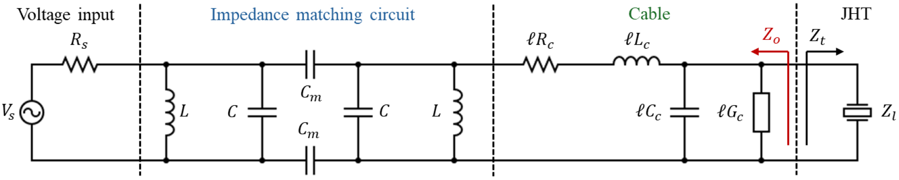
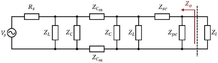
The circuits shown in Fig. 2 are rearranged into their equivalent impedance representations, as illustrated in Fig. 3. In this equivalent model, the internal resistance of the voltage source is denoted as , and the load impedance, representing the impedance of the JHT, is designated as . The cable impedance is divided into a series component and a parallel component .
Using Thevenin’s theorem,[13] the output impedance and the equivalent voltage can be derived and are expressed as follows:
where , ,.
The complex impedances of and are composed of resistance and reactance so that they can be expressed as and .
Since the load impedance consists of fixed RLC components, the load current can be expressed as follows:
where denotes a design parameter of the matching circuit.
Then, the active power at the load can be expressed as follows:
The matching circuit maximizes the by canceling the reactance through complex conjugate matching, such that . The objective function for maximizing the across the dynamic driving frequency range is defined as follows:
where denotes the normalized TVR over the target frequency band. It is employed as a weighting factor by being inversely applied to the , thereby enhancing power transfer in frequency regions where the TVR is relatively low.
By optimizing this objective function, the optimal values of , and that yield maximum effective power can be determined. To determine the optimal , and values, the Particle Swarm Optimization (PSO) algorithm was employed.[14] The PSO algorithm iteratively optimizes a population of candidate solutions, known as particles. In each iteration, particles adjust their positions based on the best solutions identified by neighboring particles within a defined neighborhood. The PSO method is particularly effective for navigating complex, non-convex, and non-smooth optimization spaces. Unlike gradient-based optimization techniques, PSO does not require derivative calculations, which are often challenging to obtain in complex valued domains. Moreover, compared to genetic algorithms, PSO demands fewer control parameters. In the present implementation, each particle, representing a candidate solution of , and , is updated at every iteration, and the input impedance is calculated using these updated parameters to evaluate the resulting active load power .
The proposed dual-resonant circuit design method, utilizing the PSO algorithm, provides a balanced solution for maximizing power transfer through impedance matching without the need for external devices, while maintaining low design complexity.
III. Simulation Results
To design the JHT and analyze its impedance characteristics, the Distributed Parameter Model (DPM) was utilized as described in Reference [3]. The axisymmetric simulation model is depicted in Fig. 4, and the corresponding structural parameters of the designed JHT are provided in Table 1. Furthermore, a 100-meter cable was modeled to replicate the electrical behavior reported in Reference [12].
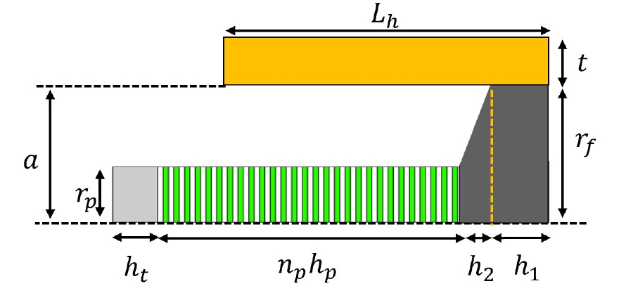
Table 1.
Structural parameters of the JHT[3].
For simulation analysis, the impedance characteristics of the load are presented in Fig. 5. In this study, resonant frequencies are defined as the frequencies at which the phase of the impedance is closest to 0°, signifying minimal reactive component. These frequencies mark the boundaries of the non-resonant region, wherein the impedance phase deviates substantially from 0°. This non-resonant region exhibits increased reactance, which causes significant phase mismatch between voltage and current, thereby reducing power transfer efficiency.
Note that the JHT has resonant frequencies at 1450 Hz and 2480 Hz, Usually, the JHT is used for frequency band between the two resonant frequencies. However, we consider two frequency bands illustrated in Fig. 6 to evaluate performance of the proposed impedance matching circuit. The first region covers wider frequency bands, including both resonant and intermediate non-resonant band. The second region corresponds to only non-resonant bands, and its bandwidth is empirically set to be 60 % of . Thus, load impedance of band has large reactance, and power transfer efficiency can be reduced. The frequency bands of two types are summarized in Table 2.
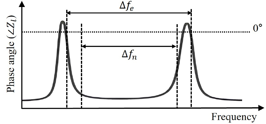
Table 2.
Frequency ranges and bandwidths.
| Band | Parameter | Range (Hz) |
| Frequency range | [1656, 2274] | |
| Bandwidth | 618 | |
| Frequency range | [1450, 2480] | |
| Bandwidth | 1030 |
The values of , and in the impedance matching circuit are determined by the PSO algorithm using Eq. (5). Table 3. summarizes the hyperparameter settings employed in the PSO algorithm. In this design, is assumed to be 50 Ω, which is typical output impedance of signal generators. To account for resistive losses caused by high-value inductors in practical applications, the convergence range of in the PSO algorithm was constrained. Based on the characteristics of a commercial component (B82731T, TDK Electronics), which exhibits a resistance of 6.6 Ω at 100 mH, the quality factor at the minimum operating frequency of 1450 Hz in this study is approximately 138, indicating sufficiently high performance. Therefore, the inductance search range in the PSO algorithm was set to 1 mH to 100 mH. For the capacitor, since the matching frequency approximates the anti-resonance, the capacitance range was chosen such that the anti-resonance frequency centers around 1965 Hz, which corresponds to the target matching band. Accordingly, the capacitance search range was defined as 1 pF to 0.15 μF. The optimized values of , and for the matching circuit, obtained using the objective function defined in Eq. (5), are presented in Table 4.
Table 3.
PSO algorithm parameters.
| Parameter | Value |
| Swarmsize | 30 |
| Inertiarange | [0.1 1.1] |
| SelfAdjustmentweight | 1.49 |
| SocialAdjustmentweight | 1.49 |
| MaxIterations | 600 |
Table 4.
Optimized coupling capacitor and inductor of the impedance matching circuit.
| Band | Parameter | Value |
| 522 nF | ||
| 22 mH | ||
| 1 pF | ||
| 625 nF | ||
| 24 mH | ||
| 1 pF |
In the simulations, performance was evaluated by comparing the average of , minimum and deviation of the TVR with and without the application of the matching circuit.
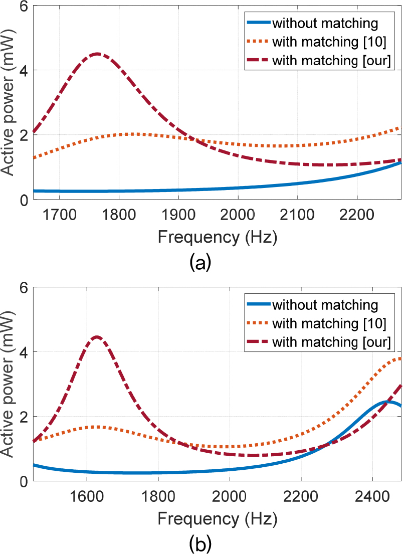
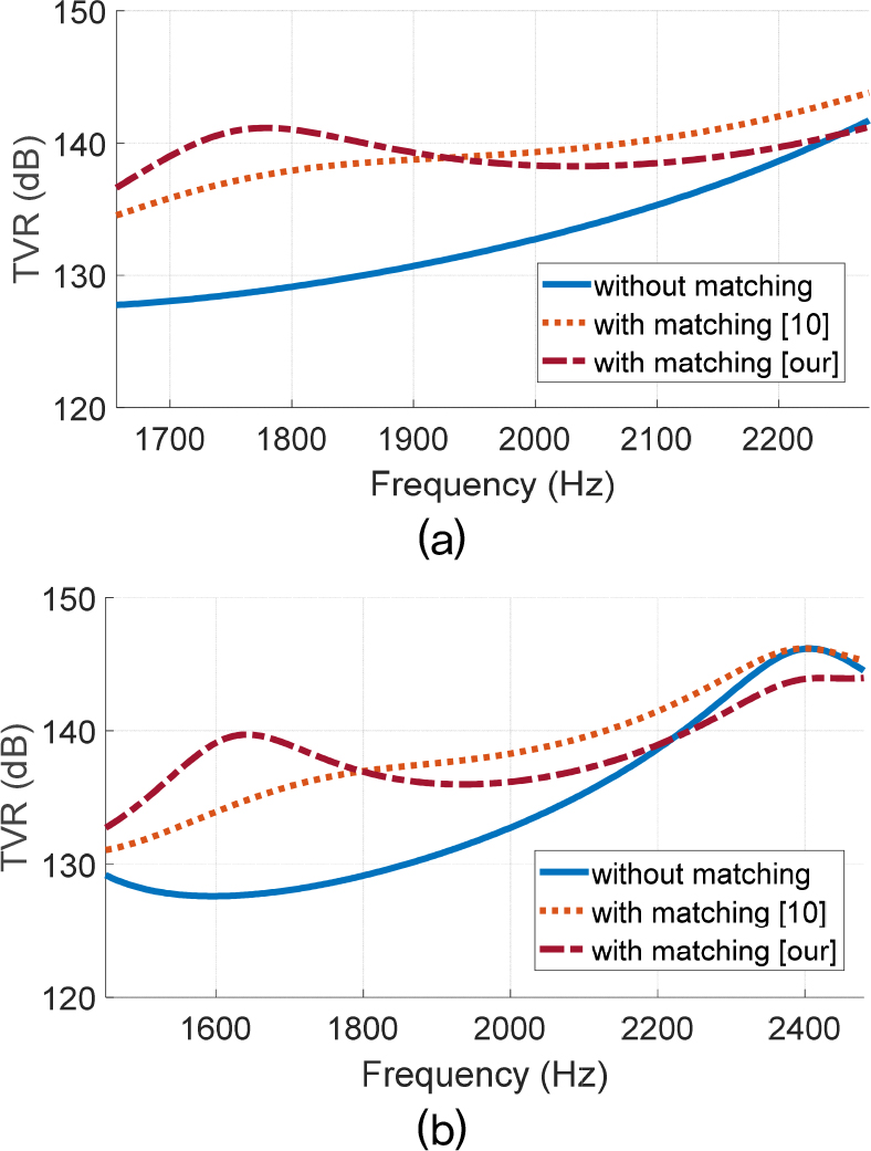
The matching circuits used for evaluation include the one from a previous study,[10] which was designed to maximize both input and load power factors, and the matching circuit proposed in this paper, which is optimized to maximize the active power delivered to the load. Fig. 7 illustrates the load power for each frequency range of and , with and without the matching circuit. The proposed matching circuit demonstrates high effective power in the non-resonant frequency band below 1,800 Hz compared to the existing method and unmatched case, where the transducer exhibits relatively low TVR performance. Table 5. summarizes the average effective power for each frequency band under the different matching conditions. In the band, the power increased from 0.72 mW to 1.79 mW, representing a 2.48 times improvement. In the narrower band, the power increased from 0.43 mW to 2.13 mW, corresponding to a 4.95 times enhancement. Fig. 8 illustrates the TVR for each frequency band with and without the matching circuit. In the non-resonant frequency band below 1800 Hz, the proposed matching circuit yields superior TVR performance compared to the conventional method, owing to enhanced power delivery in the low-TVR band. Table 6 summarizes the minimum and deviation of the TVR across each frequency band under different matching conditions. In the band, the minimum TVR increased by 8.9 dB, and the TVR deviation decreased by 9.4 dB. In the narrow band, the minimum TVR increased by 5.2 dB, while the TVR deviation was reduced by 7.4 dB. The increase in active power and TVR arises in non-resonace band from the cancellation of the load reactance by the output reactance, which is achieved through the JHT matching circuit designed according to the objective function defined in Eq. (5).
IV. Conclusions
In this study, we proposed a dual-resonance-based impedance matching circuit design method to maximize power transfer in the JHT. The proposed approach utilizes an equivalent power driving circuit that incorporates a compact matching network and is guided by an objective function targeting the maximization of effective load power. By considering the transmitting characteristics of the transducer and enabling high power transfer in the non-resonant frequency band, the proposed matching circuit improves power transfer efficiency and TVR performance. Simulation results based on an equivalent JHT circuit model indicate that, under a 1 Vrms input voltage, the average effective power delivered to the JHT reaches 2.13 mW, representing a 4.95 times improvement compared to the unmatched case. In addition, the minimum TVR increases by more than 5 dB, while the TVR deviation is reduced by over 7 dB. While the proposed matching circuit improves power transfer and TVR performance in the non-resonant frequency band, the dual-resonance-based design has inherent limitations in enhancing performance across the entire frequency spectrum. These findings suggest that future research should explore extended matching strategies beyond dual-resonance designs to further improve broadband power transfer efficiency.
